- back to top


SOLUTION
Accumulated rich experience in the research and production of high-precision, high-density, and high reliability printed circuit boards
SOLUTION
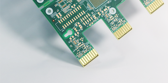
Thick copper plate process solution

Product Introduction and Process Features
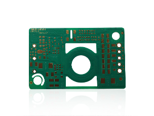
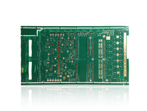
Thick copper plates are mainly high current substrates, which are generally high-power or high-voltage substrates. They are commonly used in automotive electronics, communication equipment, aerospace, network energy, planar transformers, power converters, and secondary power modules. The development of thinness and miniaturization in electronic products urgently requires PCBs to have higher thermal conductivity, and the application of thin core thick copper multilayer boards is more widespread. The advantages of thick copper: Thick copper plates (≥ 3oz) have the ability to carry large currents, reduce thermal strain, and have good heat dissipation.
Characteristics of Thick Copper Process
Etching usually involves etching twice
Special pressing program for pressing
Special resin filling treatment is required for 8oz or above (inclusive)
Welding prevention requirements
Line Mask Design
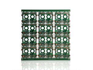
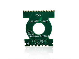
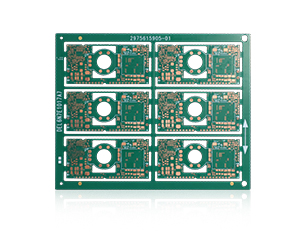
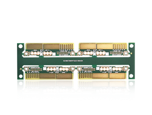
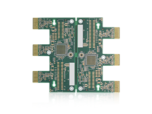
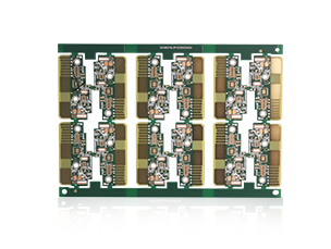
Related products

Home Page
Previous Page
1
2
3
4
Next Page
Last Page
Jiangxi Business Department:
Tel:+86 0796 8616 983
Email:wlgpcb@welgaopcb.com
Address: No. 1, Yongjin Avenue, Jinggangshan Economic and Technological Development Zone, Ji'an City, Jiangxi Province
Huizhou Business Department:
Thailand Business Department:
Tel:0752-6237000
Email:ad-m@welgaopcb.com
Address: No. 116, Jianshe Road, Longyuan Industrial Park, Mabei Town, Boluo County, Huizhou City, Guangdong Province
Official WeChat (Service Number)
Follow us
Jiangxi Weier High Electronics Co.,Ltd 赣ICP备2023012175号 Technical support:xhkj
- back to top


Official WeChat (subscription number)
Tel:095 9870 006
Email:wm.song@welgaopcb.com Address: Nong Nam Som, Uthai, Phra Nakhon Si Ayutthaya 13210
About us
Product
Solution
Contact us